


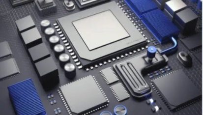
Application of Diamond in New Electronic Packaging Substrate
Release time:
2023-05-17
With the rapid development of modern microelectronics technology, electronic systems and equipment are developing in the direction of large-scale integration, miniaturization, high efficiency and high reliability. The increase in the integration of electronic systems will lead to an increase in power density and an increase in the heat generated by the overall operation of electronic components and systems. Therefore, effective packaging must solve the heat dissipation problem of electronic systems.
Good device heat dissipation depends on optimized heat dissipation structure design, package material selection (thermal interface material and heat dissipation substrate) and package manufacturing process. Among them, the selection of substrate material is the key link, which directly affects the cost, performance and reliability of the device. Generally speaking, the application of electronic packaging materials needs to consider two basic performance requirements. The first is high thermal conductivity to achieve rapid heat transfer and ensure that the chip can work stably under ideal temperature conditions; at the same time, the packaging material needs to have adjustable Thermal expansion coefficient, so as to maintain a match with the chip and all levels of packaging materials, and reduce the adverse effects of thermal stress. The development trajectory of electronic packaging materials is the continuous improvement and optimization of these two properties.
new typePackage substrateOf course, the material also needs to consider other properties, such as high resistivity, low dielectric constant, dielectric loss, good thermal matching with silicon and gallium arsenide, high surface flatness, good mechanical properties and easy industrial production. Therefore, the choice of new packaging substrate materials is a hot spot for research and development in various countries. At present, several commonly used packaging substrates are Al2O3 ceramics, SiC ceramics, AlN and other materials.
As early as 1929, the German Siemens company successfully developed Al2O3 ceramics, but the coefficient of thermal expansion and dielectric constant of Al2O3 relative to Si single crystal is high, the thermal conductivity is not high enough, resulting in Al2O3 ceramic substrate is not suitable for high frequency, high power, very large scale integrated circuit use.
Then the high thermal conductivity ceramic substrate material SiC, AlN, SI3N4,DiamondGradually enter the market.
The thermal conductivity of SiC ceramics is very high, and the higher the purity of SiC crystals, the higher the thermal conductivity; the biggest disadvantage of SiC is that the dielectric constant is too high and the dielectric strength is low, so it limits its high-frequency applications and is only suitable for low-density packaging.
AlN material has excellent dielectric properties and stable chemical properties, especially its thermal expansion coefficient is matched with silicon, which makes it a promising semiconductor packaging substrate material. However, the thermal conductivity is low, and with the increasing demand for heat dissipation in semiconductor packaging, AlN materials also have certain development bottlenecks.
In the end, diamond stands out. Diamond has good comprehensive thermophysical properties. Its thermal conductivity at room temperature is 700~2200W/(m · K), and its thermal expansion coefficient is 0.8 × 10⁻⁶/K. It has many excellent characteristics in semiconductor and optical fields, but a single diamond is not easy to make into packaging materials, and the cost is high.
According to the mixing rule, the diamond/metal matrix composites prepared by adding diamond particles to high thermal conductivity metal matrices such as Ag, Cu and Al are expected to become a new type of electronic packaging material with low thermal expansion coefficient and high thermal conductivity. Based on the excellent electrical conductivity and high thermal conductivity of copper, the diamond/copper composite material was developed as a substrate material for electronic packaging, and it was confirmed that the diamond/copper composite material has good platability and solderability, meets the performance requirements of low thermal expansion coefficient and high thermal conductivity of electronic packaging substrate material, and has lower density and lighter weight than Mo/Cu alloy, therefore, the diamond/copper composite material with diamond as the reinforcing phase and copper as the matrix material can be used for chip packaging, which can improve the performance of the electronic equipment system and help reduce the weight of the equipment.
With the materials, devices and other aspects of technical issues continue to overcome, diamond has become a set of high thermal conductivity, good heat dissipation and other advantages in a substrate material, in a higher temperature environment, is the manufacture of low power consumption, high power density devices, the best semiconductor materials, its huge potential to attract more and more researchers into it. The potential of diamond will gradually be developed to meet the needs of the semiconductor industry in the future and occupy a place in the semiconductor electronic packaging materials.
Focus on hot spots
The main application of diamond powder
Ultra-precision polishing of precision instruments for the use of nanodiamonds
Characteristics of Shandong Metal Powder Hydraulic Press
Unlocking Efficiency: The Full Digital Servo Hydraulic Press Revolution

CONTACT US
Address: east of Luxi Orthopedic Hospital, Guangyue Road, Liaocheng High-tech Industrial Development Zone